PLI International
Thermal Shock PCB
Thermal shock in the context of printed circuit boards (PCBs) refers to the sudden and extreme temperature changes that can occur during the manufacturing and testing process. These temperature changes can cause stress on the PCB and its components, leading to failures or defects.

PLI International
Thermal Shock PCB
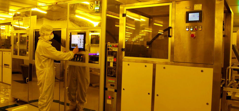
The most common cause of thermal shock in PCBs is the process of soldering components onto the board. The high temperatures used in the soldering process can cause thermal stress on the PCB and its components. This stress can cause the board to warp or crack, and can also cause the components to become dislodged or damaged.
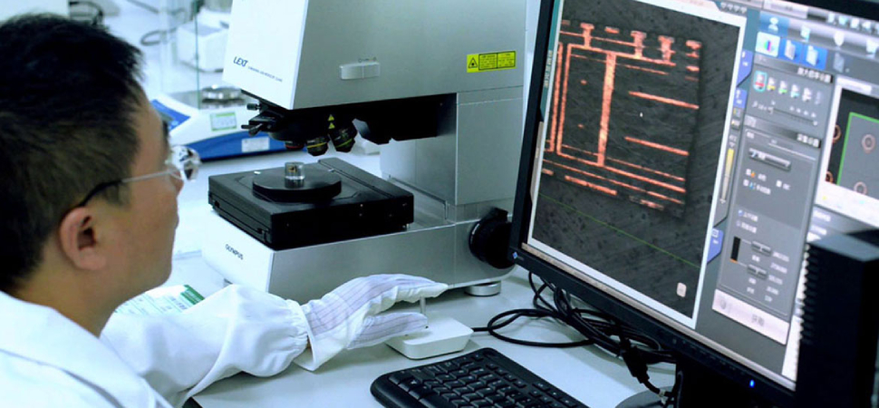
Thermal shock can also occur during testing when the PCB is exposed to temperature extremes. Testing may involve exposing the PCB to high temperatures to simulate the conditions it will experience in use. If the PCB is not able to withstand these temperature extremes, it may fail or develop defects.
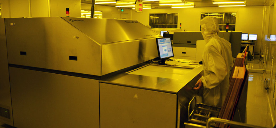
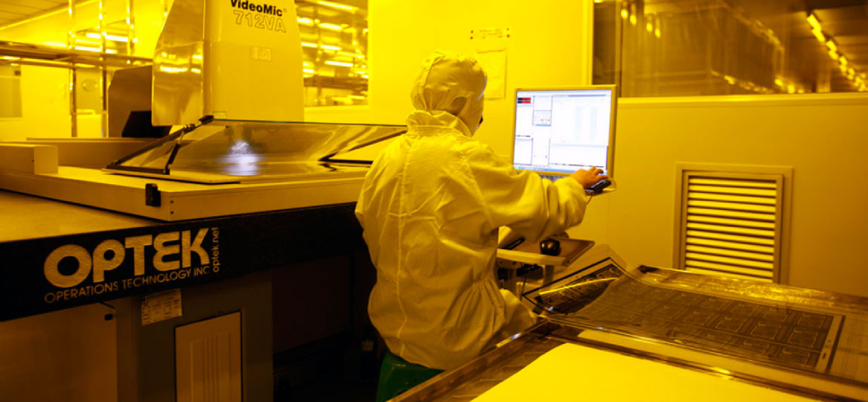
To minimize the risk of thermal shock, PCB manufacturers use a range of techniques and materials. These may include the use of specialized materials that can withstand high temperatures, such as ceramic PCB substrates. Manufacturers may also use thermal management techniques, such as heat sinks, to dissipate heat and reduce the risk of thermal stress on the PCB.
Overall, thermal shock is an important consideration in the design and manufacturing of PCBs. By taking steps to minimize the risk of thermal stress, manufacturers can improve the reliability and longevity of their products.
flex boards / HDI