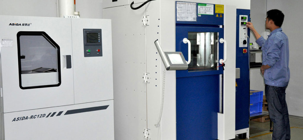
PLI International
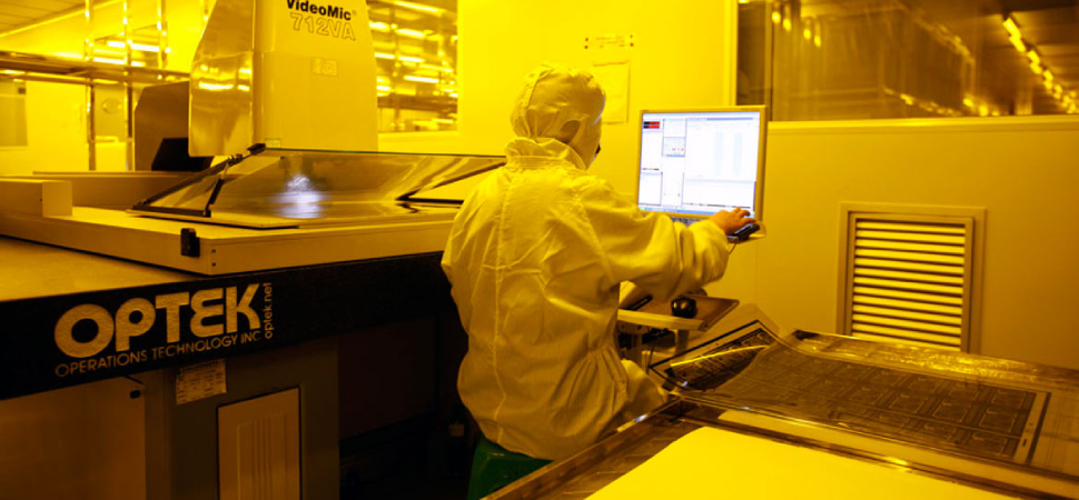
3D Microscope PCB Inspection
3D microscope PCB inspection is a method of inspecting printed circuit boards (PCBs) using a high-resolution microscope that can produce 3D images of the PCB surface. This type of inspection is used to detect defects and ensure the quality of the PCBs during the manufacturing process.

PLI International
3D Microscope Pcb Inspection
The 3D microscope uses a combination of optical and digital technologies to produce high-resolution images of the PCB surface. The microscope can capture images of the PCB from different angles, allowing for a detailed examination of the surface and any components mounted on it. The images produced by the microscope can be viewed in 3D, providing a detailed view of the PCB’s topography and any surface defects.
3D microscope inspection can detect a wide range of defects, including missing components, damaged components, misalignment of components, and solder joint defects. The microscope can also measure the dimensions of components and the spacing between them, ensuring that they meet the design specifications.
One of the main advantages of 3D microscope inspection is its ability to detect defects that may not be visible using traditional 2D inspection methods. The 3D images produced by the microscope can reveal defects that may be hidden from view, such as defects in the solder joints or under surface-mounted components.
Another advantage of 3D microscope inspection is its high accuracy and precision. The microscope can capture images with sub-micron resolution, allowing for the detection of very small defects and the measurement of very small components.
3D microscope inspection is widely used in the electronics manufacturing industry to ensure the quality of PCBs and improve the reliability of electronic products.
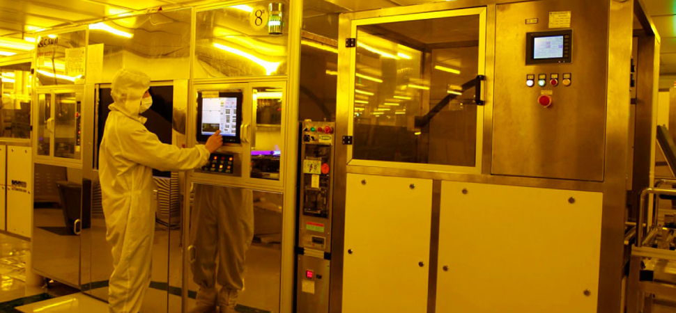
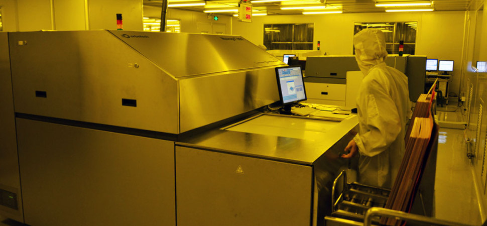
Flex Boards / HDI / Multi-Layer Boards / Rigid-Flex Boards